   |
||||||||
|
|
 |
 |
|||||||
| Defined by design architecture and transmission speed DRAM can be classified into 3 categories �V FPM (Fast Page Mode) DRAM, EDO (Extended Data Out) DRAM and SDRAM (Synchronous DRAM). Among all, FPM DRAM is the earliest development and slowest, advancing to EDO DRAM to the till so far fastest in the main stream memory market: SDRAM. After SDRAM, DRAM architecture turns to the faster DRDRAM (Direct Rambus DRAM and DDR (Double Data Rate) SDRAM. DRDRAM and the current main stream SDRAM are not popularly accepted in the market due to the big skill gap, low yielding, larger cubic and high cost of package & test which makes it difficult to lower down the equipment and production costs. Moreover there are license and copyright issues. DRDRAM are mainly used in high end platforms, early P4 initial products and in the Intel��s suppliers groups. DDR/DDR2 became main stream due to the very similar skill requirements as that of SDRAM and shares the utilization of SDRAM production equipment. Furthermore, production cost is only 10% higher than that of SDRAM and is without licensing and copyright concerns.
The PC market consistently repeats the cycle of CPU upgrades �� OS (Operating System) and more functional practical applications �� enlargement of hardware (memory) demands. Nowadays this periodical cycle will be prolonged. The computer is not the only market for the memory occupation. The consumer electronic products, internet and telecommunication market have started to grow now. |
|||||||
Since our R&D focus is on the memory field, we have innovated the PC-based DRAM test software & hardware test platform equipment ourselves as well as providing our customers full SDRAM, DDR, DDR2 customized Die & IC test services.
The accumulated experiences include:
When the memory technology turned into the 90mm and 65nm nanometer process, design techniques have stepped gradually into High Bit Density, High Speed, and Low Power requirements. The original PC test platform could no longer rely precisely on the test to meet the memory key parameter requirements due to the limitation of the BIOS & chipset architecture. Newer test platforms can accurately be adjusted to the working frequencies, voltage and current to test the DDR, DDR2, SRAM, FLASH. and other memory types meanwhile by providing a test interface for TSOP and BGA package. |
|||||||
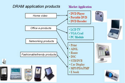
DRAM is the most popular memory device, is a mature technology and comprehensively used in all kinds of systems. Applications range from Server Workstations, Desktops, Notebook computers to Disk Controllers, network cards, Video Graphic cards and DVD players.
DRAM device trends are High bit Density, High Speed, Low Power design and
production has thus advanced to 0.13um�B0.11um�B90nm�B65nm foundry technology
 During IC memory chip testing the entire PC test procedures, practical application systems and test environments are all unalike. Actual adopted systems have different usage ranges such as PC memory modules, DVD players and routers. Integration of these systems tests becomes of essential importance. The procedure of this system test requires alteration of the adopted systematic PCB layout design and memory IC related electric circuit to increase DRAM memory IC electric circuit allowing all types of the memory IC. Then the system is switched on for direct testing on these memory IC��s to check if these ICs are acceptable. The system test is to assure that the memory IC yield is within 1% tolerance. As for partial Bin2 adoptions, the systems needs to be slightly adjusted, therefore the need for this system test is even more important. |
|||||||
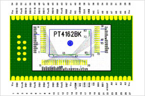
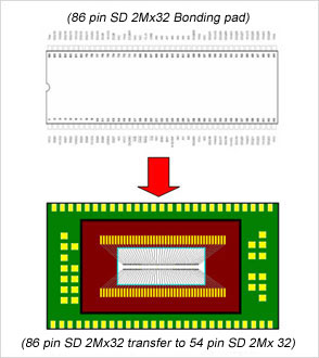
The smart package memory technology is used for the existing DRAM die and IC testing platform technology as a base for managing the memory IC pins, type, lower capacity transfer etc. to achieve cost-down of DRAM packaging cost and also to increase the flexibility of the memory capacity utilized by means of related DRAM technology, coordination on the testing software category and PCB layout and combined COB (Chip-on-board) package. High capacity and smaller cubic requirements have resulted into the BGA packaging of the DRAM IC. The characteristics are that the bonding pad will be lined up by a method by either moving toward to purely one side or to be lined up in L-shape. Through the Smart Package the die can be packaged differently and so the DRAM adoption range can be extended from hard-disk controller to DVD systems |
|||||||